Creating a Coldfire Processor Model
We are using the Coldfire Processor MCF5307. The two documents that we are using are:
We know some basic facts by looking at the block diagram:
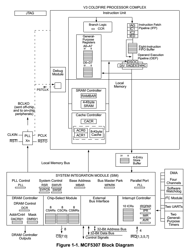
For the list of blocks in the Processor, we refer to the Block Diagram in Figure 1-1 of Document 1.

We see the Processor core, 8 Kb
cache, 4 kb SRAM, Local Memory Bus that connects to the DRAM
controller, DMA, and the I2C. It also shows 16 registers and the
pipeline.
Blocks to bring into the Editor
- Digital - This is the simulator block that manages the simulation, model debugging, and the Stop Time.
- Architecture_Setup -
Required block for all architecture work. This block maintains the
connectivity between blocks, statistics and debugging
information. This block requires no input. The statistics
can be generated for this block by connecting a Text_Display to the
second and third output port. The top port is used to plot the
list of statistics in “List of Statistics to plot” parameter of the
block. This is linked to each of the hardware blocks via the
name. Delete the entire content of the Routing_Table field. These
are automatically generated by the Model.
- Processor block - This
is the core of the processor and contains the first level (sometimes
second level cache, if available), pipeline, Execution Units, and the
instruction queue.
- Instruction_Set -
Overhead block that is not connected to any other block. This block
maintains the list of instructions for each execution unit and the
associated execution time. These are the number of cycles and is
used by the pipeline to know how much to delay the instruction.
- Linear Bus and Linear
Port - This is to add the local memory bus. Notice that there is
a 4 buffer storage from the processor core to these devices. Modify the
FIFO_Buffer size in the Linear_Port to 4. Set the Bus names in
both the Controller and Port to Memory_Bus. The Bus speed is the
baseline setting for all the other clocks. “The processor complex
frequency is an integer multiple, 2 to 4 times, of the external bus
frequency.”
- Note: For this
tutorial training, we are only going to add the DRAM, the DMA, and the
AVB Ethernet interface. Add at least two Linear_Port blocks to
the model. Note that each port has a unique name.
- DRAM - Add the DRAM
block to the right side Linear_Port. We assume a large DRAM with
a 32 bits or 4 byte wide at the bus clock speed.
- DMA - Add the DMA to
the left side of the Linear_Port. Also add the DMADatabase block.
This block maintains the association of each channel to a Task. There
is no input or output to this block. For the purpose of this
experiment connect the left side to the Processor block directly.
We assume that the processor makes the data access request. The
Linking_Table_Name must match the DMA Database Name in the DMA
block. The DMA has 4 channels. The Speed is same as the
Bus. The DMA width is the same as the Bus and is 4 bytes. There
is a 2 cycle internal access time and is entered in the DMA_to_Device
and Device_to_DMA.
- SRAM - Create two
ports (one input and one output) for the Processor core and put them on
top of the Processor. Add a DRAM block. The setting of the
DRAM block to SDR makes this block behave as a SRAM. For the
purpose of this example, this SRAM is not being used. It could be used
to store certain data and this can be modeled as an advanced feature of
the Pipeline. The SRAM is 1024*32 bits with size of 4 KB. The clock
speed is the same as the core. There is one cycle read and write
access. There is controller overhead. The local buffer at
the SRAM is 1. As this is a SRAM, we add the Refresh parameter to turn
off the Refresh. It is 32-bit and we set the width to 4 bytes. As this
is a SRAM, we need the Access_Time for the Read and Write only.
The document states - “Single-cycle throughput”. The Access_Time
is in ns. Hence we set it to Read 1000.0/Memory_Speed_Mhz, Write
1000.0/Memory_Speed_Mhz.
- Cache- List an I_1
cache internal to the Processor core. For this Cache Miss, we send the
request via the External Memory Bus to the DRAM. Notice the
configuration of the Cache inside the Processor block. Both Instruction
fetch and data access are done to this Cache block. The document
lists the following information for the “The MCF5307 processor contains
a nonblocking, 8-Kbyte, 4-way set-associative, unified (instruction and
data) cache with a 16-byte line size.” We use this to update the
parameters. The speed is the same as the Processor core.
The size is 8 KB and the Words per Cache Line = 16*8/32 (16 Bytes * 8
bits/ 32 bits)=4. The next level memory is the external DRAM.
- To get started, we shall use the Soft_Gen. Later we will add the AVB_Node block.
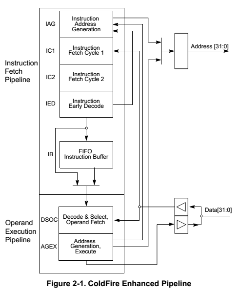
For more pipeline details, look at Figure 2-1 of Document 2.

Let us start with the pipeline.
We have 2 pipelines. The
first gets the instructions and the second gets the data, executes the
instructions, and writes the data back to the Cache. The instruction
and data accesses in the pipeline use the same I1 cache.
Pipeline 1.
- We shall create a single cycle for the generate address.
- Instruction fetch.
- Wait for Instruction return.
- Decode.
Instruction Queue or Bypass:
There is a queue between the two stages. This queue can be
bypassed if the second pipeline is available. We make an
assumption here. We have 8 additional stages between the two
pipelines. Each stage behaves as an instruction queue
position. There is a small error at startup of 7 extra cycles.
After this the pipeline is always accurate.
Pipeline 2.
- Data Fetch
- Execute
- Write back to cache
Pipeline:
Stage_Name Execution_Location Action Condition ;
1_Address
none
exec
none
;
2_FETCH
I_1
instr
none
;
3_FETCH_RET
I_1
wait
none
;
4_DECODE
I_1
wait
none
;
5_Q1
none
exec
none
;
6_Q2
none
exec
none
;
7_Q3
none
exec
none
;
8_Q4
none
exec
none
;
9_Q5
none
exec
none
;
10_Q6
none
exec
none
;
11_Q7
none
exec
none
;
12_Q8
none
exec
none
;
13_DFETCH
I_1
read
none ;
14_EXECUTE
I_1
wait
none ;
14_EXECUTE
UNIT
exec
none ;
15_STORE
UNIT
wait
none ;
15_STORE
I_1
write
none ;
Notice that we have a Wait for
Return for Instruction, data, and execution. We do not have a
wait for the Store because this must not affect the pipeline. The
stages 5-12 provide the instruction buffer. There is one cycle
delay between them. Hence we get the initial error of 8 extra
cycles.
Configuring the Processor:
Clock Speed - Multiple of the Bus Speed
Context Switching - This is variable and can be used to improve the accuracy.
Execution Unit - 4
Stages of the pipeline = 15 from above
Number of caches - 1
Number of Registers= 16+32= 16 User Registers and 32 Unallocated Registers. We do not include the Supervisory Registers.
Instruction Set Name; ColdfireInstr
Processor_Bits is the width and it is 32 bit.
DMADatabase Configuration
For this example, we have
simply assumed two Tasks that will execute on the Processor. Also
the instruction names are simply Load and Store. All the Load and
Store are done to the external DRAM only. This is defined in the
Coldfire document. The data size is assumed. The burst size
matches the Bus. The DMA has 4 channels. Each of the types are
assigned to a separate channel.
Instruction Set
The basic execution of the
Coldfire contains the standard arithmetic, logical, branch, and move
operations. In addition, there are the three Execution Units-
Multiply/Accumulate Unit (MAC), Integer Divide Module (IDM), and
Floating Point Unit (FPU). MAC is a Floating Point while IDM is
an Integer Unit. Hence, the setting in the Processor is for three
Floating Point and one Integer Execution Unit.
We have a common name for these
modules called UNIT. We associate the UNIT with the FP_1
(standard unit), FP_3 (MAC), FP_2 (FPU), and INT_1 (IDM).
STD: All standard instructions have timing information in the Table.
FPU: We have implemented FPU in this version. The user can select whether to include them in the code or not.
MAC: The list of instructions
are in Table 3-1 and the timing information are in Tables 3-2 and
3-3. We have modified some of the names so that they are concise.
IDM: DIVS and DIVU. As
these have different timing based on the data type and we use the
uniform distribution for the timing.
Operation and Data Stimulus
The incoming data from the
camera, audio or other sensors are fed into this hardware unit that
does all the Stream reservation and the Ethernet processing. If
the user wants to add additional load to each packet, simply add
additional tasks in the Instruction_Mix_Table.
Why does the actual software code not impact the performance analysis? Why is the percentage of instruction sufficient?
Ans: We have tried multiple experiments to prove this aspect. We have three variations:
- Current model.
- Disconnect the DMA activity and generate transactions to the Processor.
- Modify the percentage of instruction of each type within a task.
- Modify the pipeline to be nine stages and eliminate the extra queuing items.
Response:
- You notice that the DMA has the greatest impact. This drops the MIPS to 1.2.
- The combination of instructions in the code does have an impact and it ranges from 16-21.5 MIPS.
- Rearranging the pipeline does not have sufficient impact.

