Schmidt Trigger Circuit Design using FSM
Designing a schematic circuit design
Open this model in VisualSim from the following location:
$VS/doc/Training_Material/FSM/Trig/SchmidtTrigger.xml
Sometimes an input signal to a digital circuit does not directly fit the description of a digital signal. For various reasons it may have slow rise and/or fall times, or may have acquired some noise that could be sensed by further circuitry. It may even be an analog signal whose frequency we want to measure. All of these conditions, and many others, require a specialized circuit that will "clean up" a signal and force it to true digital shape.
The required circuit is called a Schmidt Trigger. It has two possible states just like other multi-vibrators. However, the trigger for this circuit to change states is the input voltage level, rather than a digital pulse. That is, the output state depends on the input level, and changes only as the input crosses a pre-defined threshold.
In this experiment, we look at the theory of this circuit's operation, and then build a VisualSim model to analyze the functionality and optimize the behavior.
Unlike the other multi-vibrators you have built and demonstrated, the Schmidt Trigger makes its feedback connection through the emitters of the transistors as shown in the schematic diagram to the right. This makes for some useful possibilities, as we see during our discussion of the operating theory of this circuit.
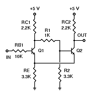
Figure 1: Schematic of a Schmidt Trigger
To understand how this circuit works, assume that the input starts at ground, or 0 volts. Transistor Q1 is necessarily turned off, and has no effect on this circuit. Therefore, RC1, R1, and R2 form a voltage divider across the 5 volt power supply to set the base voltage of Q2 to a value of (5 x R2)/(RC1 + R1 + R2). If we assume that the two transistors are essentially identical, then as long as the input voltage remains significantly less than the base voltage of Q2, Q1 will remain off and the circuit operation does not change.
Note: Classical analyzes of this circuit include the forward current gain, hFE, of the two transistors. This was important in the early days of transistors when a signal transistor was doing well to have a current gain of 30. Modern transistors have a much higher gain (160 for the 2N3904/2N3906, 200 for the 2N4124/2N4126), so they do not have the same limitations as older transistors. We can ignore the effects of transistor base current, although we do still need to account for VBE for the two transistors.
While Q1 is off, Q2 is on. Its emitter and collector current are essentially the same, and are set by the value of RE and the emitter voltage, which is less than the Q2 base voltage by VBE. If Q2 is in saturation under these circumstances, the output voltage is within a fraction of the threshold voltage set by RC1, R1, and R2. It is important to note that the output voltage of this circuit cannot drop to zero volts, and generally not to a valid logic 0. We can deal with that, but we must recognize this fact.
Now, suppose that the input voltage rises, and continues to rise until it approaches the threshold voltage on Q2's base. At this point, Q1 begins to conduct. As it now caries some collector current, the current through RC1 increases and the voltage at the collector of Q1 decreases. But this also affects our voltage divider, reducing the base voltage on Q2. But as Q1 is now conducting, it carries some of the current flowing through RE, and the voltage across RE does not change as rapidly. Therefore, Q2 turns off and the output voltage rises to +5 volts. The circuit has just changed states.
If the input voltage rises further, it keeps Q1 turned on and Q2 turned off. However, if the input voltage starts to fall back towards zero, there must clearly be a point at which this circuit resets itself. The question is, What is the falling threshold voltage? It is the voltage at which Q1's base becomes more negative than Q2's base, so that Q2 begins conducting again. However, it is not the same as the rising threshold voltage, as Q1 currently affects the behavior of the voltage divider.
We do not go through all of the derivation here, but when VIN becomes equal to Q2's base voltage, Q2's base voltage is:

As VIN approaches this value, Q2 begins to conduct, taking emitter current away from Q1. This reduces the current through RC1 which raises Q2's base voltage further, increasing Q2's forward bias and decreasing Q1's forward bias. This turns off Q1, and the circuit switches back to its original state.
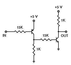
Figure 2: Circuit Diagram
Three factors must be recognized in the Schmidt Trigger. First, the circuit changes states as VIN approaches VB2, not when the two voltages are equal. Therefore VB2 is very close to the threshold voltage, but is not precisely equal to it. For example, for the component values shown above, VB2 is 2.54 volts when Q1 is held off, and 2.06 volts as VIN is falling towards this value.
Second, as the common emitter connection is part of the feedback system in this circuit, RE must be large enough to provide the requisite amount of feedback, without becoming so large as to starve the circuit of needed current. If RE is out of range, the circuit does not operate properly, and may not operate as anything more than a high-gain amplifier over a narrow input voltage range, instead of switching states.
The third factor is the fact that the output voltage cannot switch over logic levels, as the transistor emitters are not grounded. If a logic-level output is required, which is usually the case, we can use a circuit such as the one shown here to correct this problem. This circuit is basically two RTL inverters, except that one uses a PNP transistor. This works because when Q2 above is turned off, it holds a PNP inverter off, but when it is on, its output turns the PNP transistor on. The NPN transistor here is a second inverter to re-invert the signal and to restore it to active pull-down in common with all of our other logic circuits.
The circuit you construct for this experiment includes both of the circuits shown here, so that you can monitor the response of the Schmidt trigger with L0.
A modal model of a Schmidt trigger is developed in VisualSim. The output from the Schmidt trigger moves from -1.0 to 1.0 when its input becomes greater than 0.3, and moves back to -1.0 after its input becomes less than -0.3.
4. In this Editor
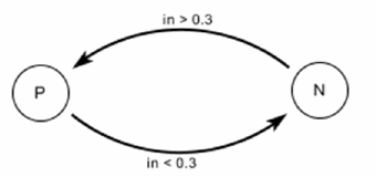
Figure 3: VisualSim State Machine Diagram
Figure 4: VisualSim Model of the Refinement States
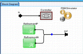
Figure 5: Schmidt Trigger Hierarchical FSM
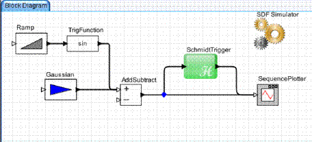
Figure 6: Top-Level VisualSim Block Diagram
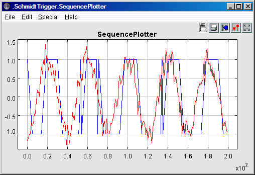
Figure 7: Results of the Schmidt Trigger model