Multi-Chiplet Interconnect Performance Analysis
Objective: The objective of this experiment is to analyze the performance dynamics and data transfer efficiency of a multi-chiplet interconnect system through simulation. Students will engage with the interconnect architecture, including CPU, GPU, DSP, AI, and IO chiplets, to understand how these elements interact and contribute to the system’s overall performance and data throughput.
Location: https://www.mirabilisdesign.com/launchdemo/demo/Bus_Std/UCIe/UCIe_Chiplet/
Overview: This simulation model provides a hands-on experience for examining the impact of interconnect architectural choices on performance and data transfer efficiency. With detailed components like chiplet communication pathways, debugging tools, and a network-on-chip (NoC) router, students can observe real-time changes in data transfers, emphasizing the critical role of interconnects in modern processor design.
Experimental Setup:
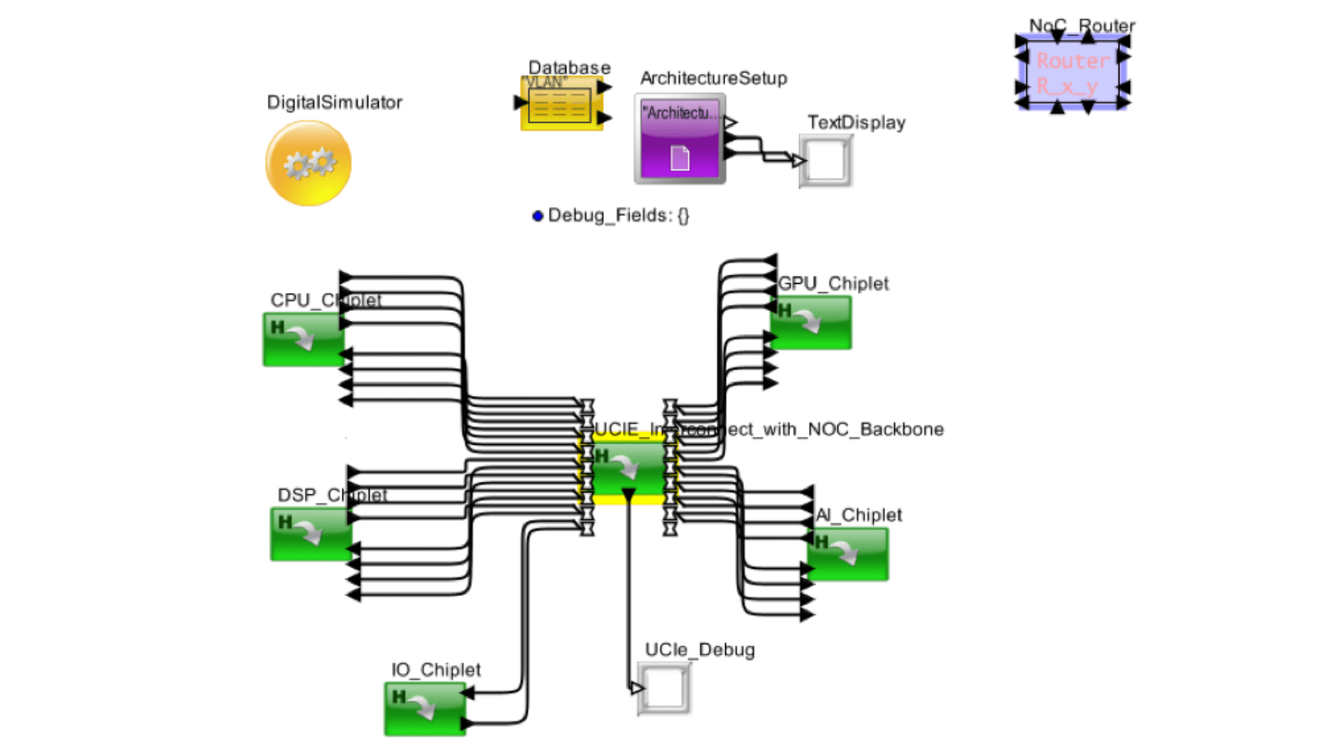
Base Experiment: This experiment features a multi-chiplet interconnect system characterized by various chiplets each with specific processing capabilities. The system uses a UCle interconnect with an NoC backbone to manage data transfer between chiplets. The following configuration is used:
- CPU Chiplet: Handles general processing tasks.
- GPU Chiplet: Manages graphical processing tasks.
- DSP Chiplet: Dedicated to digital signal processing tasks.
- AI Chiplet: Specialized in artificial intelligence computations.
- IO Chiplet: Manages input/output operations.
- UCle Interconnect with NOC Backbone: Facilitates communication between chiplets.
This setup provides a framework for evaluating the performance of multi-chiplet interconnects under various computational loads, emphasizing the interplay between interconnect efficiency and overall system performance.
Notes to consider while performing the tasks:
- Record all simulation parameters and modifications accurately
- Analyze the impact of changes on key performance metrics, such as data throughput and latency.
- Consider and document the trade-offs between different interconnect configurations.
- Explore and document additional modifications to enhance the system’s performance.
- Thoroughly document observations, findings, and conclusions for each simulation run.
Task 1: Changing Package Type and Simulation.
We will change the package type from Standard to Advanced and observe the impact on performance.
Procedure for Modification:
- Access the UCle Interconnect configuration block within the simulation software.
- Locate the parameter labeled Package_Type: Standard.
- Change this value from Standard to Advanced.
Task 2: Increasing Maximum Link Speed and Simulation.
We will increase the maximum link speed from 32 GT/s to 64 GT/s.
Procedure for Modification:
- Access the UCle Interconnect configuration block within the simulation software.
- Locate the parameter labeled Max_Link_Speed_GTPs.
- Change all the values from 32 to 64.
Task 3: Adjusting Buffer Size for Transmission (Tx) and Simulation
We will increase the buffer size for transmission (Tx) from 4096 bytes to 8192 bytes.
Procedure for Modification:
- Access the UCle Interconnect configuration block within the simulation software.
- Locate the parameter labeled Buffer_Size_Bytes: 4096.
- Change this value from 4096 to 8192.
Simulation and Analysis:
- Run Simulation for Each Task: Start the simulation for each task separately.
- Monitor Outputs: Use the TextDisplay block to monitor outputs and results from the simulation.
- Document Results: Record the results for each parameter change and analyze the impact on performance and data transfer efficiency.
Challenging Questions:
- How does changing the package type from Standard to Advanced affect the maximum data transfer rate and overall system performance?
- What implications might increasing the maximum link speed from 32 GT/s to 64 GT/s have on data throughput and latency?
- How does adjusting the buffer size for transmission (Tx) from 4096 bytes to 8192 bytes influence the performance and efficiency of data transfers between chiplets?
- What could be the potential trade-offs when modifying these parameters in a multi-chiplet interconnect system?
RSIC-V SMID Experiment
Objective: The objective of this experiment is to analyze the operational dynamics and power efficiency of a RISC-V processor system through simulation. Students will engage with the processor’s architecture, including the pipeline, cache, and memory components, to understand how these elements interact and contribute to the system’s overall performance and power consumption.
Location: https://www.mirabilisdesign.com/launchdemo/doc/Training_Material/Architecture/Processor/RISC_V/RISC_V_Inorder/
Overview: This RISC-V Processor System simulation provides a hands-on experience for examining the impact of architectural choices on performance and power efficiency. With detailed components like in-order execution, dual cache layers, and DMA, students can observe real-time changes in processing tasks, emphasizing the critical role of cache and memory management in modern processor design.
Experimental Setup:
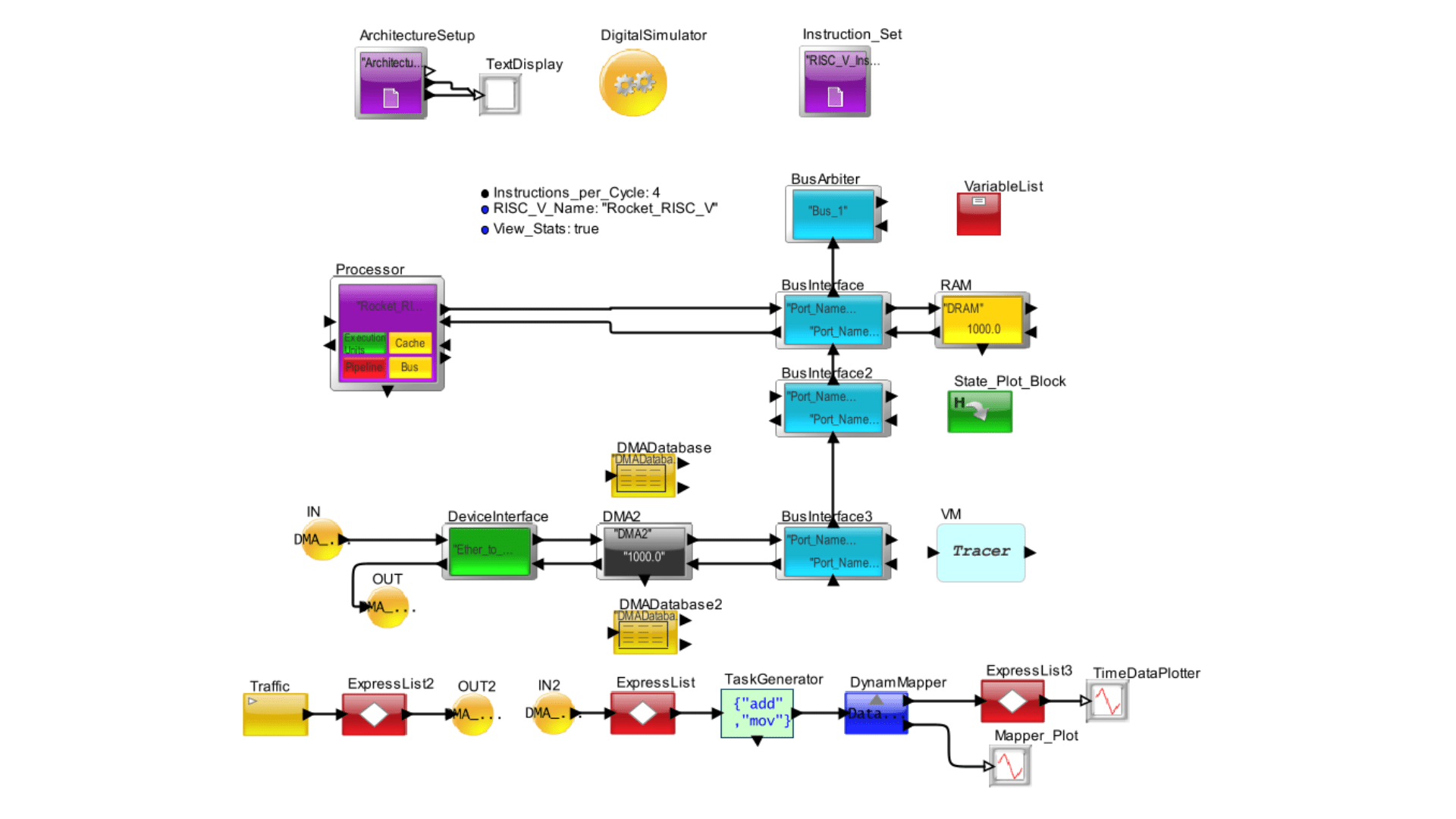
Base Experiment:
This experiment features a RISC-V based processor characterized by a comprehensive instruction set where each instruction’s execution time is meticulously defined. The processor is equipped with a single integer execution unit that supports basic arithmetic operations: addition and subtraction are executed in 1 cycle, multiplication and division each require 4 cycles, and jump operations take 3 cycles.
The processor operates at a clock speed of 1 GHz (1000 MHz) and incorporates a 32-register architecture. It features a 4-stage pipeline design, optimizing the flow of instructions through the execution unit. Context switching is notably efficient, with a cycle count of 200.
For memory, the processor is exclusively equipped with Level 1 instruction and data caches (L1 I-cache and L1 D-cache), both operating at a speed of 500 MHz. Each cache has a capacity of 16 KB, tailored to ensure rapid data access and minimize latency.
This setup provides an efficient framework for evaluating the performance of RISC-V processors under various computational loads, emphasizing the interplay between processor speed, pipeline architecture, and caching systems.
Results:
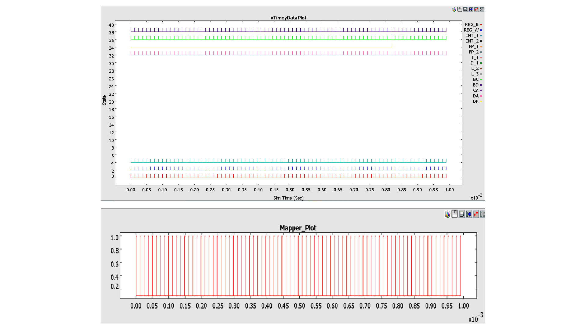

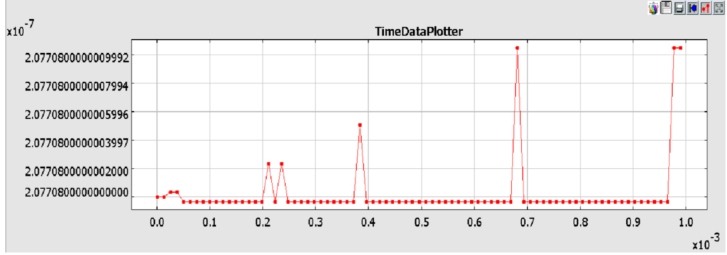
Task 1: Pipeline Stage Reduction and Simulation
As part of the ongoing evaluation of our RISC-V based processor, we will modify the pipeline architecture. The current configuration consists of four pipeline stages. The objective is to streamline this setup by reducing the number of stages to three.
Procedure for Modification:
- Access the processor configuration block within the simulation software.
- Locate the parameter labeled Number_of_Pipeline_Stages: 4.
- Change this value from 4 to 3 to reflect the new pipeline stage configuration.
Revised Pipeline Stages:
- First Stage (Fetch): This stage is responsible for fetching the instruction from the instruction memory.
- Second Stage (Decode and Execute): This newly combined stage will handle both the decoding of the fetched instruction and its execution. Combining these functions into a single stage aims to optimize the transition between interpreting and executing the commands.
- Third Stage (Store): The final stage will manage the storage of the results of execution back into memory.
Challenging Question:
- How does reducing the number of pipeline stages from 4 to 3 affect the maximum pipeline utilization?
- What implications might the reduction of pipeline stages have on context switching and overall performance?
- Why might combining the decode and execute stages into one pipeline stage result in improved processor resource management?
- What could be the potential trade-offs when reducing pipeline stages in a RISC-V processor’s architecture?
DNN Model Mask R-CNN CPU Experiment
Objective: To evaluate the performance and efficiency of dynamically instantiating Deep Neural Network (DNN) models on the VisualSim Architect platform. This involves analyzing the impact of dynamic allocation of resources on throughput, latency, and power consumption in a hardware-software co-simulation environment.
Location: https://www.mirabilisdesign.com/launchdemo/demo/DNN/DNN_Model_Mask_R_CNN_CPU/index.html
Overview: The experiment entails designing a DNN model workflow on VisualSim Architect, incorporating dynamic instantiation of layers and resources based on workload demands. By simulating the DNN model’s execution on the target hardware architecture, we aim to quantify the benefits and trade-offs of dynamic instantiation compared to static allocation strategies. This experiment will enable us to assess the feasibility and effectiveness of dynamic instantiation as a technique for optimizing DNN inference on resource-constrained hardware platforms.
Base Experiment:
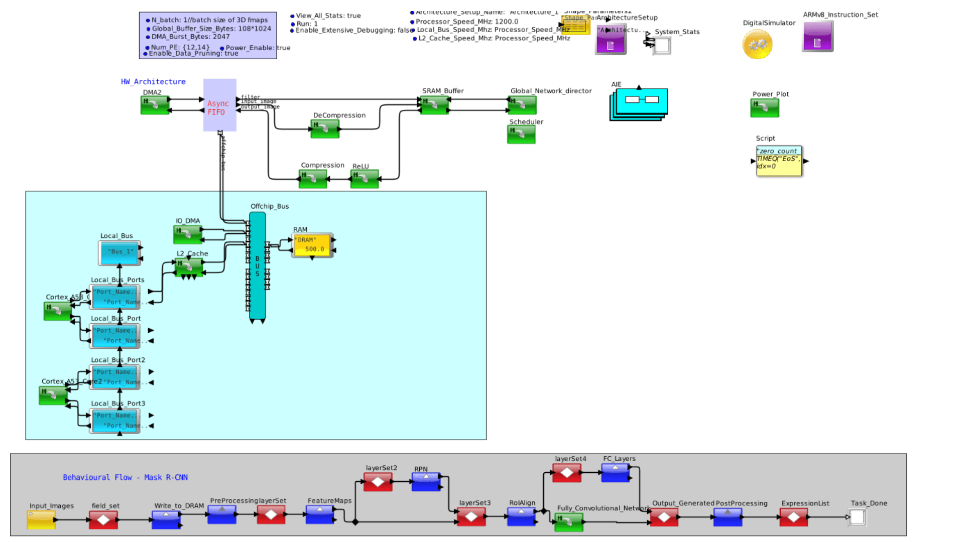
Base model:168 AI Cores, 90% data availability at SRAM
AI_Cores: Num_PE = {12, 14} // Initialize parameters
Cache_Hit_Expression = “rand(0.0, 1.0) <= 0.9” // Data availability in the SRAM (cache block)
Results:
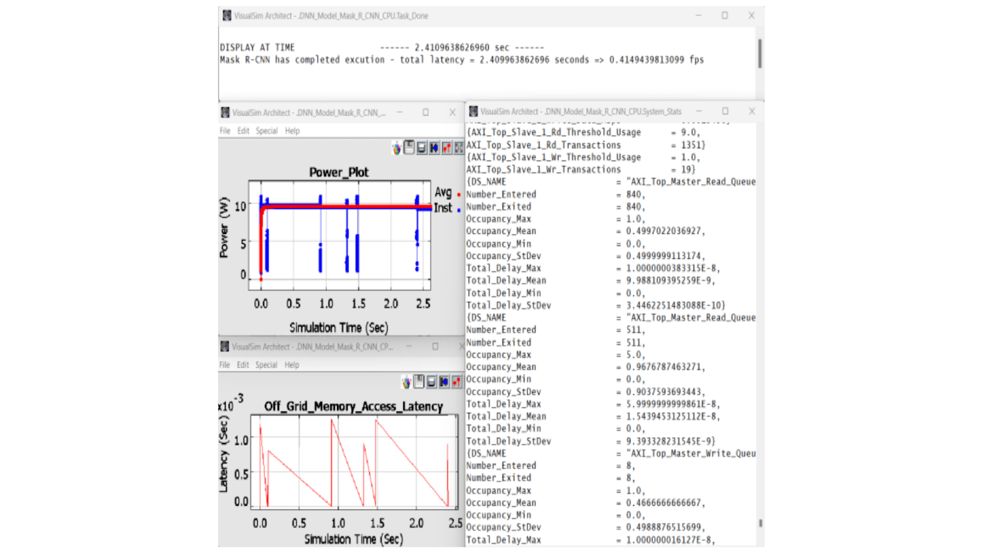
- Peak Power consumption at around 10.8 Watts Obtained FPS = 0.414
Notes to remember:
- Record all simulation parameters and modifications.
- Analyze the impact of changes on performance metrics (e.g., execution time, power consumption).
- Consider the trade-offs between different architectural choices.
- Document observations, findings, and conclusions thoroughly.
Task 1: Set up and configure a system with 64 cores (8×8) ensuring 90% data availability in SRAM.
Change the Num_PE = {8,8}
Cache_Hit_Expression = “rand (0.0, 1.0) <= 0.9” // Data availability in the SRAM block
Task 2: Set up and configure a system with 168 cores ensuring 100% data availability in SRAM.
Change the Num_PE= {12,14}
Cache_Hit_Expression = “rand (0.0, 1.0) <= 1.0” // Data availability in the SRAM block
Task 3: Set up and configure a system with 168 cores ensuring 60% data availability in SRAM.
Change Num_PE = {12,14}
Cache_Hit_Expression = “rand(0.0, 1.0) <= 0.6” // Data availability in the SRAM block
Challenging Questions:
- What were the primary resource bottlenecks observed during the experiment, and how did they impact the overall performance of the DNN model?
- In what specific scenarios did dynamic allocation of resources outperform static allocation, and what were the key factors contributing to this difference?
- How did the dynamic instantiation of DNN layers affect power consumption? Were there any trade-offs observed between performance gains and increased power usage?
- If the DNN model complexity or the input data size were significantly increased, how would the dynamic instantiation approach need to be adapted to maintain optimal performance?
- What are the practical implications of these findings for deploying DNN models on resource-constrained edge devices or embedded systems?