AMD-Xilinx VisualSim Versal SoC-FPGA App Explorer is a high level stochastic model of the FPGA-SOC devices to provide architects and system integrators with the ability to experiment with partitioning the signal processing application onto the Versal devices. The Versal device has multiple resources including ARM Cortex A72 processor, ARM R5F real-time processors, programmable logic, and an AI Engine array. This system model will help legacy FPGA application architects to complete the initial partitioning definition of applications onto the heterogeneous compute resources available in the Versal device at an optimal performance-power-area.
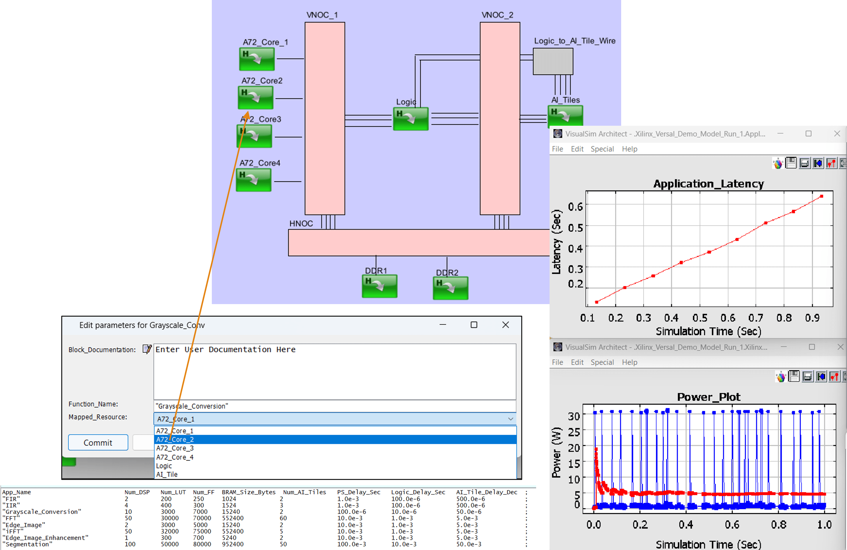
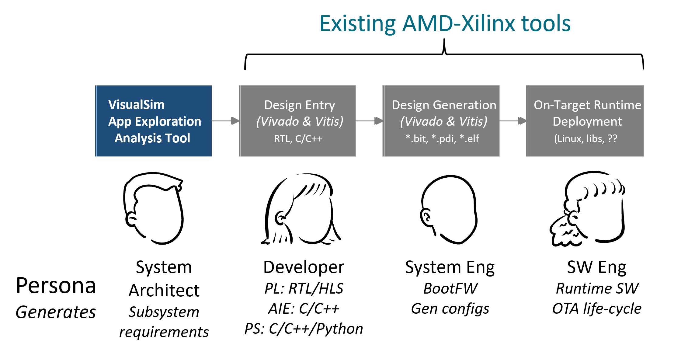
This Exploration platform enables MatLab users and architects to quickly experiment different mappings and fabric configurations to arrive at the optimal assignment of algorithms to the Versal resource. The optimization will be based on a variety of factors including power consumed, latency, throughput and resource usage. The built-in requirements monitor AI Engine identifies performance bottlenecks, causes of the bottlenecks, deadlocks and other anomalies. The App Explorer is used prior to data entry in Virtis, Vivado and MatLab.
The designer can quickly trade-off
- Learn how the #Processor, Logic Elements and AIE/Tensor are interconnected using Network-on-Chip- NoC (Horizontal and Vertical).
- What is the #latency when using the NoC vs direct interface to go between Logic->AIE or Processor and the #AIE?
- How does different data cache size requirements affect the utilization of the AIE Tile network?
- How does different mapping decisions affect the throughput of the application?
This modeling and simulation platform provides the full family of Versal device. This platform contains the all the
- Hardware IP components
- Functional blocks to map, handle data transfer and memory accesses for the tasks of the algorithms
- Timing, resource usage and power details for the list of pre-defined signal processing function
- A set of templates and tutorials provide a quick start for new users
- Traffic generators for the workload and the interface data input
The models will be assembled using building blocks that will combine functionality, power, and timing. The model is split into two flows- the standard Versal library component that represents the hardware architecture and the sequence of functional blocks that represent the application. The applications will be triggered using events and the functional blocks are a sequence of math/signal processing functions. Each math function will identify key parameters and a compute resource to be mapped to (PS, PL or AIE). All the timing, power and functional details of the compute resources, the interconnects, NoC, interfaces and memory accesses for both DDR and HBM are integrated into the Versal model. The Network-on-Chip will send data to the memory, which will include the DDR controller, HBM and memory model. The math functions will be mapped to one of PS, PL, or AIE. The transition between math functions will depend on the prior function and the next function.
The VisualSim AMD-Xilinx has a lookup table for the timing, resource used and power details of the math functions on the heterogeneous resources. The connectivity between the different types of compute resources has both a direct path and NoC. The Versal has traffic generators to simulate the data input on all the interfaces, which can be varied for rates and sizes. The internal IP blocks include the NoC, AXI buses, DMA, external interfaces, processors, logic (LUT, FF, DSP), AI Engine tiles, multiple Memory Controllers, DDT4/5 and HBM.
The user can generate a number of debugging sequences and a list of responses to different use-cases and test scenarios. In addition, there are standard reports for
- latency and throughput race across each device for a single algorithm flow
- Latency to complete a algorithm sequence
- Memory and NoC throughput by use-case
- Average, power and cumulative power for each resource, memory and for the entire Versal
- Resource utilization of the PS, PL and AIE
Advanced users can expand the scope of the architecture trade-offs by expanding the models to including other components at the board and chassis level to define the full electronics product. Example of product built using this approach can be a router, security appliance, industrial and automotive platforms, and other multimedia devices. Within VisualSim Architect, designers can select the right architecture by conducting rapid and extensive performance trade-offs during the product definition phase.
Unlike verilog/VHDL and schematic solutions that require detailed knowledge of the device, the VisualSim models can contain pre-configured components with pre-built models. These models are at a transaction-level and can be customzied by the user with minimal effort. The model of a large and complex can be constructed in a matter of a few days.
Xilinx ESL Initiative
This Xilinx FPGA Toolkit has been built in partnership with Xilinx and is targeted at developers of high-performance, high-availability products that use Xilinx FPGA products. Mirabilis Design is a member of the Xilinx ESL Initiative. The Xilinx partnership will provide FPGA and System designers a significant architecture exploration solution that increases confidence in the architecture and eliminate design bottlenecks.
<!–
Product
The product is built on top of the industry-standard VisualSim Architect. The FPGA Toolkit can be used in conjunction with the application-specific, processing functions, resource and architecture elements available in VisualSim. The modeling components provided in the FPGA library have been configured to represent the IP, cores and Fabric resources. This includes the parameters, list of standard statistics output and possible connectivity options. A list of the important toolkit components are:
–>
- Platforms (Virtex 4 and 5 Family)
- Processors/Cores (PowerPC and MicroBlaze)
- Bus and Controllers (CoreConnect- PLB and OPB, Fast Simplex Link Bus, DDR and DMA)
- Memory (SDRAM, SRAM, Block RAM and Cache)
- Communication Devices (Ethernet, PCI and PCI-Express)
<!–
Benefits
VisualSim FPGA Toolkit can identify design bottlenecks, gain greater coverage of the exploration over spreadsheets and validate your architecture prior to implementation. Using VisualSim means that Architects and Designers do not have to make simplistic assumptions using spreadsheets or spend a lot of time developing detailed C models. They can get the detailed results and accuracy of a cycle-accurate and message accurate C-model using a model that can be controlled using a spreadsheet. Architecture exploration, prior to implementation, will guarantee that your design will work the first, meet the customer requirements and can be manufactured without significant problems. All of these ensure that you have the highest quality product, at the optimal price, required performance and lowest possible power consumption.
Use Model
The Xilinx FPGA Toolkit is intended to be used by engineers that need to implement complex protocols, processing intensive application and controllers on FPGAs. The simulation can study how the FPGA will perform when different application sequence or user-input is provided. Also, the interaction between multiple FPGAs, ASIC-FPGA, and system components and FPGA can be studied. This Toolkit can be used throughput the product development process. Major design phases include early hardware and software architecture design phase; changes made to the architecture due to the requirements changing; implementation verification; and product testing.
–>